")
")
")


")

Due to the application of semiconductors in the computer industry and photovoltaics in devices such as transistors, lasers and solar cells, finding new semiconductor materials and improving existing materials is an important research field in material science.
The most commonly used semiconductor materials are crystalline inorganic solids. These materials are classified according to the periodic table groups.
Different semiconductor materials differ in their properties. Therefore, compared to silicon, complex semiconductors have both advantages and disadvantages.
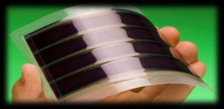
For example, Gallium arsenide (GaAs) is six times more mobile than silicon, allowing faster operation; wider area slot, allowing operation of source equipment at high temperatures. Its direct band gap gives it more favorable photovoltaic properties than the indirect band gap of silicon. Besides, it can be alloyed into tertiary and quaternary components, with adjustable slot wavelengths, and allowing to fit the step wave with the lowest loss in fiber.
In contrast, silicon is hard, cheap and easy to handle, while GaAs is fragile, expensive and insulation classes cannot be created by only a layer of oxide. Therefore, GaAs is used when silicon is not enough.
By alloying many compounds, some semiconductor materials are adjustable, for example, in a slot or network constant. The result is a creation of tertiary, quaternary or quinary compositions
The trisomy component allows adjustment of the region slot within the relevant binary compounds; however, in the case of a combination of direct and indirect slot materials, there is a proportion in which the indirect slot zone dominates, limiting the range that can be used for photoelectrons; For example, AlGaAs LEDs are limited to 660 nm in this way.
The network constant of the compounds also has different trends, and the network mismatch (mismatch) with the substrate, depending on the mixing ratio, causes quantitative defects depending on the magnitude of the mismatch; This affects the rate of recombination of radiation / non-radiation (radiative/nonradiative) achieved and determines the luminous efficiency of the device.
Quadratic and higher components allow for simultaneous adjustment of region and network constants, allowing for increased luminous efficacy at a wider range of wavelengths; For example, AlGaInP is used for LED. Transparent materials with a wavelength of light are advantageous, as this allows the separation of photons from most materials more efficiently.
In such transparent materials, the production of light is not only limited to the surface, the index of refraction also depends on the composition and affects the efficiency of photon separation from the material.
Currently, Hamamatsu (Japan) and Epitaxx (USA) can produce mid-infrared spectral range.
The IOFFE University of Russian Academy of Sciences, St. Petersburg, Russia is the leading institute of physics in Russian Federation, has successfully developed high-speed photodiode (up to 2-5 MHz) based on GaInAsSb / AlGaAsSb solid solution for spectrum 1, 6-2.4 microns, and long-wave photodiode working at room temperature based on Inas / InAsSbP is for infrared wave band 2-5 micron.
Organizational Capacity to implement
A.F. Institute of Engineering Physics Ioffe is the leading institute in the world for new semiconductor materials based on A3B5. Therefore, the implementation of the project is very urgent.
VinIT Institute of Technology is a partner of A.F. Ioffe institute. Therefore, the ability to coordinate research and technology transfer in this field is potential.
Objectives
- Create new A3B5 semiconductor materials using nano-epitaxial technology for the electronics industry;
- Developing high quality human resources.
Expected products
- Overview report and analysis of patent information for semiconductor materials;
- Reports on the properties, structure of AIGaN materials, AIGaN development, mid-infrared photodiode properties;
- 10 mid-infrared photodiode types of high-speed battery base on heterojunction slot narrow semiconductor region A3B5.
Application possibilities
The result of creating A3B5 mid-infrared photodiodes will be the technological revolution in infrared photodiode field, which can be applied in the manufacture of many electronic devices, as well as in many special fields.